BT-SFP-G05-BU05-55 SFP Module
BT-SFP-G05-BU05-55 is a high performance, cost effective modules, which is supporting up to 1.25Gbps, and transmission distance up to 500m on MM fiber. The transceiver consists of two sections: The transmitter section incorporates a laser driver and a 1550nm FP laser. The receiver section consists of a PIN photodiode integrated with a transimpedance preamplifier (TIA) and a Limitting Amplifier. The module is hot pluggable into the 20-pin connector. The high-speed electrical interface is based on low voltage logic, with nominal 100Ohms differential impedance and AC coupled in the module.
The optical output can be disabled by LVTTL logic high-level input of TX_DIS. Transmit Fault (Tx_Fault) is provided to indicate that the module transmitter has detected a fault condition related to laser operation or safety. Loss of signal (RX_LOS) output is provided to indicate the loss of an input optical signal of receiver. A serial EEPROM in the transceiver allows the user to access transceiver monitoring and configuration data via the 2-wire SFP Management Interface. This interface uses a single address, A0h, with a memory map divided into a lower and upper area. Basic digital diagnostic (DD) data is held in the lower area while specific data is held in a series of tables in the high memory area.
Features
- Up to 500m transmission on MMF
- Up to 1.25 Gbps
- 1550nm FP laser and PIN receiver
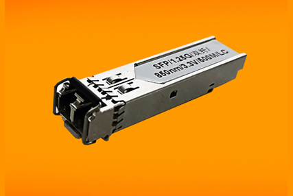
- Single LC/SC receptacle optical interface compliant
- 2-wire interface for integrated Digital Diagnostic monitoring
- Hot pluggable
- Very low EMI and excellent ESD protection
- +3.3V power supply
- Power consumption less than 1.0W
- Operating case temperature: 0~+70°C
Applications
- High-speed storage area networks
- Computer cluster cross-connect
- Custom high-speed data pipes
Compliance
- Compliant with IEEE802.3ah 1000Base-BX
- Compliant with MSA SFF-8472
- Compliant with SFP MSA
Specification
|
Absolute Maximum Ratings |
|||||
|
Parameter |
Symbol |
Min. |
Max. |
Unit |
Notes |
|
Storage Temperature |
TS |
-40 |
+85 |
℃ |
|
|
Supply Voltage |
VCC3 |
0 |
3.6 |
V |
|
|
Relative Humidity |
RH |
5 |
+85 |
% |
Note1 |
|
Rx Input Average Power |
Pmax |
- |
+1 |
dBm |
|
Notes:
- Non-condensing
|
Recommended Operating Conditions |
|||||
|
Parameter |
Symbol |
Min. |
Typical |
Max. |
Unit |
|
Operating Case Temperature |
TC |
0 |
25 |
+70 |
℃ |
|
Power Supply Voltage |
VCC3 |
3.13 |
3.3 |
3.47 |
V |
|
Total Supply Current |
ICC3 |
- |
- |
300 |
mA |
|
Power Dissipation |
PD |
- |
- |
1.0 |
W |
|
Data Rate |
1.25 |
Gbps |
|||
|
Transmitter Operating Characteristic-Optical, Electrical |
||||||
|
Parameter |
Symbol |
Min. |
Typical |
Max. |
Unit |
Note |
|
Centre Wavelength |
λC |
1500 |
1550 |
1580 |
nm |
|
|
Spectral Width |
Δλ |
4 |
nm |
FP (RMS) |
||
|
Average Optical Power |
Pavg |
-9 |
- |
-3 |
dBm |
MMF |
|
Laser Off Power |
Poff |
- |
- |
-40 |
dBm |
|
|
Extinction Ratio |
ER |
8.2 |
- |
- |
dB |
|
|
Operating Data Rate |
- |
1.25 |
- |
Gbps |
||
|
Optical Eye Mask |
Compliant with 802.3ah eye masks when filtered |
|||||
|
Tx Input Diff. Voltage |
VI |
500 |
- |
2400 |
mV |
|
|
Tx Fault Output Voltage -- Low |
VoL |
-0.3 |
- |
0.4 |
V |
|
|
Tx Fault Output Voltage -- High |
VoH |
2.4 |
- |
Vcc+0.3 |
||
|
Receiver Operating Characteristic-Optical, Electrical |
||||||
|
Parameter |
Symbol |
Min. |
Typ. |
Max. |
Unit |
Note |
|
Center Wavelength |
λr |
1260 |
1310 |
1620 |
nm |
|
|
Receive Sensitivity In Average Power |
Psen |
- |
- |
-21 |
dBm |
|
|
Los Assert |
LosA |
-35 |
- |
- |
dBm |
|
|
Los Dessert |
LosD |
- |
- |
-22 |
dBm |
|
|
Los Hysteresis |
LosH |
0.5 |
- |
-6 |
dB |
|
|
Overload |
Pin |
- |
- |
-3 |
dBm |
|
|
Rx Output Diff Voltage |
Vo |
370 |
- |
2000 |
mV |
|
|
Operating Data Rate |
- |
- |
1.25 |
- |
Gbps |
|
|
Digital Diagnostic Functions |
|||||
|
Parameter |
Symbol |
Min. |
Max. |
Unit |
Note |
|
Temperature monitor absolute error |
DMI_Temp |
-3 |
3 |
℃ |
Over operating temp |
|
Laser power monitor absolute error |
DMI_TX |
-3 |
3 |
dB |
|
|
RX power monitor absolute error |
DMI_RX |
-3 |
3 |
dB |
|
|
Supply voltage monitor absolute error |
DMI_VCC |
-3% |
+-3% |
V |
|
|
Bias current monitor absolute error |
DMI_Ibias |
-10% |
10% |
mA |
|
|
Control and Status I/O Timing Characteristics |
|||||
|
Parameter |
Symbol |
Min. |
Max. |
Unit |
Note |
|
TX Disable Assert Time |
t_off |
- |
100 |
µs |
Note1 |
|
TX Disable Negate Time |
t_on |
- |
2 |
ms |
Note2 |
|
Time to initialize including reset of TX_Fault |
t_init |
- |
300 |
ms |
Note3 |
|
TX Fault Assert Time |
t_fault_on |
- |
1 |
ms |
Note4 |
|
TX Fault Reset Time |
t_reset |
10 |
- |
µs |
Note5 |
|
LOS Assert Time |
t_loss_on |
- |
100 |
µs |
Note6 |
|
LOS Deassert Time |
t_loss_off |
- |
100 |
µs |
Note7 |
Notes:
- Time from rising edge of TX Disable to when the optical output falls below 10% of nominal
- Time from falling edge of TX Disable to when the modulated optical output rises above 90% of nominal
- From power on or negation of TX Fault using TX Disable
- Time from fault to TX fault on
- Time from TX fault to TX nominal
- Time from LOS state to RX LOS assert
- Time from non-LOS state to RX LOS
Pin-out Definition

Pin Assignment
|
Pin |
Logic |
Symbol |
Name/Description |
Note |
|
1 |
|
VeeT |
Module Transmitter Ground |
|
|
2 |
LVTTL-O |
TX_Fault |
Module Transmitter Fault |
|
|
3 |
LVTTL-I |
TX_Disable |
Transmitter Disable; Turns off transmitter laser output |
|
|
4 |
LVTTL-I/O |
SDA |
2-wire Serial Interface Data Line (Same as MOD-DEF2 as defined in the INF-8074i) |
|
|
5 |
LVTTL-I/O |
SCL |
2-wire Serial Interface Clock (Same as MOD-DEF1 as defined in the INF-8074i) |
|
|
6 |
|
MOD_ABS |
Module Absent, connected to VeeT or VeeR in the module |
|
|
7 |
LVTTL-I |
RS0 |
Not used |
|
|
8 |
LVTTL-O |
RX_LOS |
Receiver Loss of Signal Indication (In FC designated as RX_LOS, in SONET designated as LOS, and in Ethernet designated at Signal Detect) |
|
|
9 |
LVTTL-I |
RS1 |
Not used |
|
|
10 |
|
VeeR |
Module Receiver Ground |
|
|
11 |
|
VeeR |
Module Receiver Ground |
|
|
12 |
CML-O |
RD- |
Receiver Inverted Data Output |
|
|
13 |
CML-O |
RD+ |
Receiver Non-Inverted Data Output |
|
|
14 |
|
VeeR |
Module Receiver Ground |
|
|
15 |
|
VccR |
Module Receiver 3.3 V Supply |
|
|
16 |
|
VccT |
Module Transmitter 3.3 V Supply |
|
|
17 |
|
VeeT |
Module Transmitter Ground |
|
|
18 |
CML-I |
TD+ |
Transmitter Non-Inverted Data Input |
|
|
19 |
CML-I |
TD- |
Transmitter Inverted Data Input |
|
|
20 |
|
VeeT |
Module Transmitter Ground |
|
Block Diagram of Transceiver

Transmitter Section
The transmitter converts 1.25Gbit/s serial PECL or CML electrical data into serial optical data compliant with the 1000BASE-LX standard. An open collector compatible Transmit Disable (Tx_Dis) is provided. A logic “1,” or no connection on this pin will disable the laser from transmitting. A logic “0” on this pin provides normal operation. The transmitter has an internal automatic power control loop (APC) to ensure constant optical power output across supply voltage and temperature variations. An open collector compatible Transmit Fault (Tx_Fault) is provided. TX_Fault is a module output contact that when high, indicates that the module transmitter has detected a fault condition related to laser operation or safety. The TX_Fault output contact is an open drain/collector and shall be pulled up to the Vcc_Host in the host with a resistor in the range 4.7-10 kΩ. TX_Disable is a module input contact. When TX_Disable is asserted high or left open, the SFP module transmitter output shall be turned off. This contact shall be pulled up to VccT with a 4.7 kΩ to 10 kΩ resistor
Receiver Section
The receiver converts 1.25Gbit/s serial optical data into serial PECL/CML electrical data. An open collector compatible Loss of Signal is provided. Rx_LOS when high indicates an optical signal level below that specified in the relevant standard. The Rx_LOS contact is an open drain/collector output and shall be pulled up to Vcc_Host in the host with a resistor in the range 4.7-10 kΩ, or with an active termination. Power supply filtering is recommended for both the transmitter and receiver. The Rx_LOS signal is intended as a preliminary indication to the system in which the SFP is installed that the received signal strength is below the specified range. Such an indication typically points to non-installed cables, broken cables, or a disabled, failing or a powered off transmitter at the far end of the cable.
Recommended Interface Circuit

Dimensions Unit:mm
LC Receptacle

SC Receptacle

Digital Diagnostic Memory Map

Notice
Performance figures, data and any illustrative material provided in this data sheet are typical and must be specifically confirmed in writing by Born before they become applicable to any particular order or contract. In accordance with the Born policy of continuous improvement specifications may change without notice. The publication of information in this data sheet does not imply freedom from patent or other protective rights of Born or others. Further details are available from any Born sales representative.