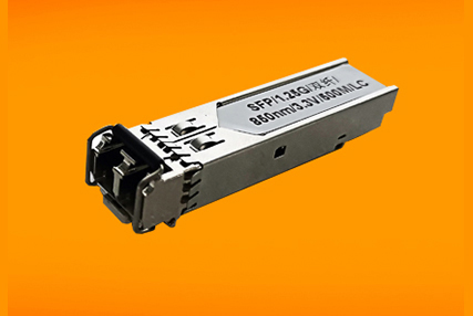
1250Mbps 1310nm Multi-Mode 2km SFP Transceiver BT-SFP-G2M
The transceiver is a low power, high performance, cost effective module supporting data-rate up to 1.25Gbps/1.0625Gbps and 2km transmission distance. The low jitter and high sensitivity are extinguished features with 1310nm FP laser and PIN/TIA receiver. It incorporates TX_DIS control, TX-FAULT and RX_LOS monitor functions. The devices are Class I laser safety compliant.
Applications
- Gigabit Ethernet
- Switch to switch interface
- 1X Fiber Channel
- Switched backplane applications
- Router/Server interface
- Other optical links
Feature
- Compliant with IEEE 802.3z
- Compliant with SFP MSA
- Up to 1.25Gbps data rate
- 2km transmission with 50/125um MMF
- 1310nm FP LD and PIN photodetecto
Absolute Maximum Ratings
|
Parameter |
Symbol |
Min. |
Max. |
Unit |
|
Storage Temperature |
Tst |
-40 |
+85 |
°C |
|
Storage Relative Humidity |
RHS |
- |
95 |
% |
|
Supply Voltage |
Vcc |
0 |
6 |
V |
|
Voltage on any input/output pin |
VIO |
0 |
VCC |
V |
Operation Environment
|
Parameter |
Symbol |
Min. |
Max. |
Unit |
|
Supply Voltage |
VCC |
3.1 |
3.5 |
V |
|
Ambient Operating Temperature |
TA |
0 |
70 |
°C |
Performance Specification
|
Transmitter Characteristics |
||||||
|
Parameter |
Symbol |
Min. |
Typ. |
Max. |
Unit |
Note |
|
Supply Voltage |
VCC |
3.1 |
3.3 |
3.5 |
V |
|
|
Differential Input Voltage |
VIN |
400 |
- |
1600 |
mV |
|
|
Data Rate |
Rate |
- |
1.25 |
- |
Gbps |
1 |
|
Rate |
- |
1.0625 |
- |
Gbps |
2 |
|
|
Optical Output Power |
Po |
-15 |
- |
-8 |
dBm |
|
|
Extinction Ratio |
ER |
9 |
- |
- |
dB |
|
|
Central Wavelength |
|
1270 |
1310 |
1355 |
nm |
|
|
RMS Spectral Width |
|
- |
- |
3 |
nm |
|
|
Optical Rise/Fall Time |
Tr /Tf |
- |
- |
0.26 |
ns |
3 |
|
Eye Diagram |
IEEE 802.3z and ANSI Fibre Channel Compliant |
|||||
|
Receiver Characteristics |
||||||
|
Parameter |
Symbol |
Min. |
Typ. |
Max. |
Unit |
Note |
|
Supply Voltage |
VCC |
3.1 |
3.3 |
3.5 |
V |
|
|
Differential Output Voltage |
VOUT |
400 |
- |
2000 |
mV |
4 |
|
Data Rate |
Rate |
- |
1.25 |
- |
Gbps |
1 |
|
Rate |
- |
1.0625 |
- |
Gbps |
2 |
|
|
Sensitivity |
S |
- |
- |
-22 |
dBm |
5 |
|
Optical Input Overload |
POL |
0 |
- |
- |
dBm |
|
|
Central Wavelength |
|
1100 |
- |
1600 |
nm |
|
|
LOS (Loss of Signal) |
Optical Decreased |
-35 |
- |
- |
dBm |
|
|
Optical Increased |
- |
- |
-23 |
dBm |
|
|
|
LOS Hysterics |
PH |
0.5 |
- |
5 |
dB |
|
Notes:
- Gigabit Ethernet
- 1X Fiber Chanel 20%~80%
- Internally AC coupled.
Average received power where the BER = 10 -12, measured with a 27-1 NRZ test pattern.
Pin Descriptions
|
Pin |
Name |
Description |
Plug Sequence |
Note |
|
1 |
VEET |
Transmitter Ground |
1 |
|
|
2 |
TX Fault |
Transmitter Fault Indication |
3 |
1 |
|
3 |
TX Disable |
Transmitter Disable |
3 |
2 |
|
4 |
MOD-DEF2 |
Module Definition 2 |
3 |
3 |
|
5 |
MOD-DEF1 |
Module Definition 1 |
3 |
3 |
|
6 |
MOD-DEF0 |
Module Definition 0 |
3 |
3 |
|
7 |
Rate Select |
Not Connected |
3 |
|
|
8 |
LOS |
Loss of Signal |
3 |
4 |
|
9 |
VeeR |
Receiver Ground |
1 |
|
|
10 |
VeeR |
Receiver Ground |
1 |
|
|
11 |
VeeR |
Receiver Ground |
1 |
|
|
12 |
RD- |
Inverse Received Data Out |
3 |
5 |
|
13 |
RD+ |
Received Data Out |
3 |
5 |
|
14 |
VeeR |
Receiver Ground |
1 |
|
|
15 |
VccR |
Receiver Power |
2 |
|
|
16 |
VccT |
Transmitter Power |
2 |
|
|
17 |
VeeT |
Transmitter Ground |
1 |
|
|
18 |
TD+ |
Transmit Data In |
3 |
6 |
|
19 |
TD- |
Inverse Transmit Data In |
3 |
6 |
|
20 |
VeeT |
Transmitter Ground |
1 |
|
Notes:
- TX Fault is an open collector output, which should be pulled up with a 7k~10kΩv resistor on the host board to a voltage between 2.0V and Vcc+0.3V. Logic 0 indicates normal operation; logic 1 indicates a laser fault of some kind. In the low state, the output will be pulled to less than 0.8V.
- TX Disable is an input that is used to shut down the transmitter optical output. It is pulled up within the module with a 7k~10kΩ resistor. Its states are:
-
Low (0~0.8V): Transmitter on (>0.8V, <2.0V): Undefined High (2.0~3.5): Transmitter Disabled
Open: Transmitter Disabled
- MOD-DEF 0, 1, 2 are the module definition They should be pulled up with a 4.7k~10kΩ resistor on the host board. The pull-up voltage shall be VccT or VccR.
MOD-DEF 0 is grounded by the module to indicate that the module is present MOD-DEF 1 is the clock line of two wire serial interface for serial ID
MOD-DEF 2 is the data line of two wire serial interface for serial ID
- LOS is an open collector output, which should be pulled up with a 4.7k~10kΩ resistor on the host board to a voltage between 0V and Vcc+0.3V. Logic 0 indicates normal operation; logic 1 indicates loss of signal. In the low state, the output will be pulled to less than 0.8V.
- LOS is an open collector output, which should be pulled up with a 4.7k~10kΩ resistor on the host board to a voltage between 0V and Vcc+0.3V. Logic 0 indicates normal operation; logic 1 indicates loss of signal. In the low state, the output will be pulled to less than 0.8V.
- These are the differential transmitter inputs. They are AC-coupled, differential lines with 100Ω differential termination inside the
Power Supply
The Transceiver includes internal circuit components to filter power supply noise. Under some conditions of EMI and power supply noise, external power supply filtering may be necessary. If receiver sensitivity is found to be degraded by power supply noise, the filter network illustrated in the following figure may be used to improve performance. The values of the filter components are general recommendations and may be changed to suit a particular system environment. Shielded inductors are recommended.
Notice
Performance figures, data and any illustrative material provided in this data sheet are typical and must be specifically confirmed in writing by Born before they become applicable to any particular order or contract. In accordance with the Born policy of continuous improvement specifications may change without notice. The publication of information in this data sheet does not imply freedom from patent or other protective rights of Born or others. Further details are available from any Born sales representative.

